Blog más reciente
Investigación sobre el método de trabajo en frío de la fuente de láser ultravioleta
Aug 22 , 2022Research on Cold Working Method of Ultraviolet Laser
At present, with the development of electronic products in the direction of portability and miniaturization, the demand for miniaturization of circuit boards is increasing. For example, modern cell phone and digital camera circuit boards have approximately 1200 interconnects per square centimeter. The key to improving the miniaturization of circuit boards is that the line width is getting narrower and the micro-aperture between different wires is getting smaller and smaller. Small vias, in order to effectively ensure the electrical connection between layers and the fixation of external devices, when designing high-speed and high-density PCBs, designers hope that the PCB vias are as small as possible, which not only leaves more wiring. space, and the smaller the via is, the more suitable it is for high-speed circuits. In this way, high-speed connection between the surface mount device and the signal board below can be achieved, and the area can be effectively reduced. PCB (PCB) has gradually formed an accumulation and multi-functionality characterized by high-density interconnection technology. Today, microvias generally account for 30%-40% of the cost of a PCB board. The minimum size of conventional mechanical drilling machines is 100 microns, which obviously cannot meet the requirements. It is a new type of laser processing method. Currently, industry requirements for micro via devices are only 30-40 microns. In addition, because the current research and development cycle for electronic products is getting shorter and shorter, in order to meet the fast and single requirements of the circuit board in the development stage, the designer requires the equipment to have the functions of punching, circuit pattern engraving and cutting. Now, foreign laser micro-hole equipment with these functions is very expensive.
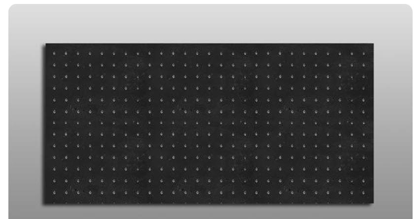
En la producción industrial, existen dos aplicaciones principales de los microagujeros láser:
1. Uso de un láser infrarrojo: una sustancia que calienta y evapora la superficie de un material para eliminar el material, comúnmente conocido como tratamiento térmico. Principalmente con CO2 (longitud de onda 10,6 micras) o láser Nd:YAG (longitud de onda 1,064 micras).
2. Láser ultravioleta: el enlace molecular de la sustancia se rompe directamente, de modo que la molécula y la sustancia se separan. Este proceso no genera mucho calor, por lo que se denomina trabajo en frío. El láser UV-YAG (355nm.266nm.213nm) se utiliza principalmente en el láser UV-YAG. En la actualidad, la tecnología de procesamiento térmico con láser infrarrojo ha sido ampliamente utilizada, pero todavía hay muchas investigaciones sobre los métodos de procesamiento en frío con láser ultravioleta. Dadas las numerosas ventajas de los láseres UV, muchas empresas de todo el mundo utilizan láseres UV.