Blog más reciente
Logotipo de placa de circuito electrónico de marcado láser de nanosegundos UV de 355 nm, fecha, gráfico
Aug 15 , 2022Logotipo de placa de circuito electrónico de marcado láser de nanosegundos UV de 355 nm , fecha, gráfico
Laser marking has a wide range of penetration in the field of electronic manufacturing, from common PCBs and FPCs to capacitors, resistors, memory, chips, etc. on circuit boards. Laser marking is used to obtain high-quality, high-contrast, high-efficiency logos and numbers. , production date, assembly line, warehouse and other graphic marks are not uncommon.
Compared with traditional screen printing technology and traditional marking methods such as labeling, laser marking is incomparable with its fast marking speed, environmental protection, strong firmness, anti-counterfeiting traceability and flexible operation. In view of the development trend of electronic components towards precision, refinement and batchization, when marking electronic components with 355nm ultraviolet nanosecond laser, it also has the characteristics of "cold" processing, high marking resolution and narrow line width. The realization of these characteristics is inseparable from the key data of the laser itself.
355nm UV light - "cold" processing. 355nm ultraviolet light can be absorbed by most metal and non-metal materials, and the wavelength is short, and the single photon energy is higher. When 355nm ultraviolet light is used for marking, it can easily break the molecular bonds of the material and separate the surface molecules from the material. This process does not generate high heat, so it is called "cold" processing. For soft and hard circuit boards and component materials commonly used in electronic manufacturing, 355nm ultraviolet light is friendly.

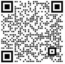
Excellent beam quality - high resolution, narrow linewidth. As the components are getting smaller and smaller, the area that can be marked is becoming more and more limited, 355nm ultraviolet light is easy to focus, and the laser beam quality is high (M2 < 1.2), the focused spot diameter is micron, and the marking line width can be 0.08 to 0.2mm, so it is possible to mark images and texts less than 1mm on the surface of components. The extremely fine light spot is more advantageous in marking the QR code. The resolution of the marked QR code is very high, which can be easily scanned and identified. At the same time, manufacturers can use the QR code to achieve product traceability and anti-counterfeiting functions.

Además, la alta flexibilidad y el procesamiento sin contacto del marcado láser también permiten la fabricación electrónica. Por un lado, la alta flexibilidad se refleja en que las marcas gráficas y de texto se pueden cambiar a voluntad a través del software de dibujo, y la variable de número de serie que se puede saltar, la variable de fecha y hora que se puede cambiar con el estándar del sistema. El tiempo, etc. se puede configurar de forma flexible. También se puede marcar uniformemente; la ventaja del procesamiento sin contacto es que no genera estrés mecánico, por lo que los componentes están libres de presión y daños, lo que a su vez afecta la facilidad de uso y la seguridad de los productos y mejora el rendimiento.