Por qué el mercado de PCB puede impulsar el crecimiento de los láseres UV de nanosegundos de alta potencia
Aug 23 , 2022Why the PCB market can bring growth momentum to high-power nanosecond UV lasers
In 2019, the growth rate of the laser processing market has further slowed down. The maturity of some application markets and the competition in the Red Sea have also caused related companies to face the dilemma of increased operating pressure and declining performance. The new crown pneumonia epidemic in 2020 has given the development of laser companies. overshadowed. In such an environment, OFweek Laser Network found that the laser market related to PCB processing is still growing. In the data disclosed by some listed companies, PCB business orders have become the main driving force supporting performance growth. How is the development of the PCB market? And why can it bring huge growth momentum to laser companies?
Rapid development of PCB and FPC industry, huge market increment
PCB is the abbreviation of Printed Circuit Board. It is one of the important components of the electronics industry and is used in almost all electronic products. Its main function is to realize the electrical interconnection between various components. The PCB consists of an insulating base plate, connecting wires and pads for assembling and soldering electronic components, and has the dual functions of a conductive circuit and an insulating base plate. Its manufacturing quality can directly affect the reliability of electronic products. It is the basic industry of today's electronic information product manufacturing, and it is also the industry with the largest output value in the current global electronic component subdivision industry.
The application market of PCB is very wide, including consumer electronics, automotive electronics, communications, medical, military, aerospace and so on. At present, the rapid development of consumer electronics and automotive electronics has become the main field of PCB applications. For a long time, the global PCB output value was mainly concentrated in North America, Europe and Japan. After 2000, the focus of the PCB industry began to shift to the Asian region, especially the Chinese market. In 2009, the output value of the PCB industry in mainland China accounted for about 1/3 of the world's total. By 2017, it had reached 50.5%, accounting for half of the global PCB output value.
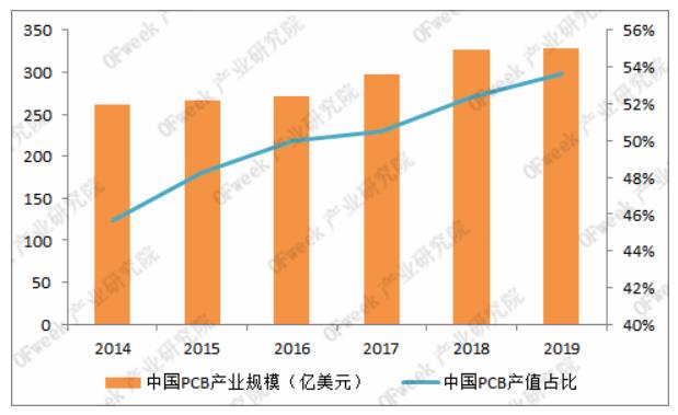
Data source: Prismark, OFweek Industrial Research Institute
In 2019, affected by trade frictions, declining terminal demand and exchange rate depreciation, the global PCB output value declined slightly, but the Chinese market benefited from the rapid development of 5G, big data, cloud computing, artificial intelligence, Internet of Things and other industries, becoming the only one in 2019. growing area. According to Prismark data, the size of China's PCB market in 2019 was about US$32.9 billion, accounting for 53.7% of the world.
In the PCB application of consumer electronics, FPC develops the fastest, and its proportion in the PCB market continues to increase. FPC is the abbreviation of Flexible Printed Circuit, which is a highly reliable and reliable product made of polyimide (PI, also known as PI cover film in the industry) or polyester film as the base material. It is an excellent flexible printed circuit board with the characteristics of high wiring density, light weight, thin thickness and good bendability. Under the current trend of intelligent, light and thin mobile electronic products, FPC is widely used due to its advantages of high density, light weight, thin thickness, bending resistance, flexible structure, high temperature resistance, etc. the only solution.
The rapidly developing PCB market has fostered a huge derivative market. With the development of laser technology, laser processing has gradually replaced the traditional die-cutting process and has become an important part of the PCB industry chain. Therefore, in the context of the slowdown in the overall growth rate of the laser market, the PCB-related business can still maintain high growth.
The advantages of laser in PCB and FPC processing
The application of laser on PCB mainly includes cutting, drilling, marking, etc., especially cutting. Compared with the traditional die-cutting process, laser cutting is a non-contact process, without the need for expensive molds, and the production cost is greatly reduced; in addition, the traditional process is difficult to solve a series of problems such as burrs, dust, stress, and inability to process curves on the edge. The laser spot is only ten microns after focusing, which can meet the processing requirements of high-precision cutting and drilling, and solve a series of problems left in the traditional process. This advantage is catering to the development trend of precision circuit design, and it is an ideal tool for PCB, FPC, PI film cutting.
In fact, the application of PCB laser cutting technology in the PCB industry started earlier, but CO2 laser cutting was used in the early stage, which has a large thermal impact and low efficiency, and has not been able to achieve good development. It is only used in some special fields (such as scientific research , military, etc.) are used. With the development of laser technology, more and more light sources can be used in the PCB industry, and a breakthrough has been found for the industrial application of laser cutting PCB.
Currently, the lasers used in FPC and PI film cutting are mainly nanosecond solid-state UV lasers, and the wavelength is generally 355nm. Compared with 1064nm infrared and 532nm green light, 355nm UV has higher single-photon energy, higher material absorption rate, less thermal impact, and higher processing accuracy.
From a principle point of view, pulsed laser cutting materials can be divided into two situations: one is the photochemical principle, using the single photon energy of the laser to reach or exceed the chemical bond energy of the material to break some chemical bonds of the material to achieve cutting; the other is the light According to the physical principle, when the laser single photon energy is lower than the chemical bond energy of the material, the very high energy density at the focused spot exceeds the gasification threshold of the material, thereby instantly gasifying the material and realizing the cutting of the material. But in fact, when cutting FPC or PI film with UV laser, the principles of photochemical and photophysical cutting exist at the same time.
The following two processing principles are explained by taking PI film as an example. The bond energy of C-C bond and C-N bond in normal state is 3.45eV and 3.17eV respectively, while the single-photon energy of 355nm UV laser is 3.49eV, which is higher than that of C-C bond and C-N bond in normal state It can directly destroy the chemical bonds of materials. (Reference: Zhang Fei, Duan Jun, Zeng Xiaoyan, et al. Research on 355nm ultraviolet laser processing of blind vias in flexible circuit boards [J]. China Laser, 2009, 36(12):3143-3148.)
In the photophysical effect, there will be heat generation and accumulation, and the temperature of the material will continue to rise. When the temperature of the PI material is higher than 600 °C, the ratio of N and O elements will continue to decrease relative to the C element, and the final material is mainly dominated by the C element, that is, the material is carbonized. The diffusion distance formula L=[4Dt]^1/2, where D is the thermal diffusivity of the material, and t is the laser pulse width. (Reference: Zhang Peng, Chi Weidong, Shen Zengmin. Influence of high temperature carbonization on the structure and properties of polyimide (PI) thin films [J]. Carbon Technology, 2008, 27(6):10-12.)
It can be seen that when the material is constant, the larger the laser pulse width, the larger the diffusion distance of the thermal energy generated by the laser on the material, and the greater the thermal damage to the material. Therefore, the narrower the pulse width, the better the processing effect.
20W/25W nanosecond UV laser: higher power, better effect
As mentioned above, my country's PCB industry has benefited from the rapid development of emerging industries such as 5G and big data. The emergence of new industries and new technologies has also put forward higher requirements for the FPC and PI film cutting industries. In order to achieve less carbonization and faster efficiency, laser companies are also constantly making technological innovations, and constantly exploring higher frequencies, narrower pulse widths, and higher powers.
¿Qué tipo de cambios puede traer el nuevo láser UV de nanosegundos de ancho de pulso corto de alta frecuencia al procesamiento de PCB? A continuación se muestran algunos casos de procesamiento
Corte de dedos de oro
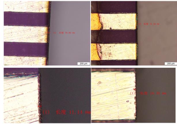
AWAVE 15W @50KHZ efecto de corte, velocidad efectiva: 50mm/s (izquierda)
FORMULA 15W @150KHZ efecto de corte, velocidad efectiva 100mm/s (derecha)
En comparación con el láser de la serie AWAVE tradicional, el efecto de corte del láser de la serie FORMULA mejora significativamente y la eficiencia de corte también se ha mejorado en un 100%.
Perforación de láminas de cobre
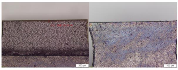
Frontal (izquierda) Posterior (derecha)
Perforando agujeros en la lámina de cobre con un espesor de 100um, la eficiencia del láser de la serie FORMULA de 20W es un 60% superior a la del 15W, alcanzando los 250 mm/s.
corte de placa de circuito impreso
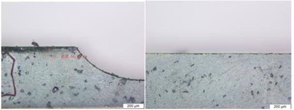
Frontal no borrado (izquierda) Reverso no borrado (derecha)
Para el corte de PCB con un espesor de 400um, la eficiencia del láser de la serie FORMULA de 20W es un 50% superior a la de 15W, alcanzando los 60mm/s.
Corte de tableros de refuerzo FPC
Frontal (izquierda) Posterior (derecha)
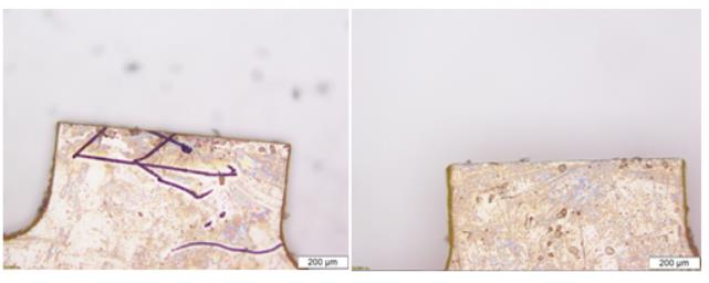
Para cortar placas reforzadas con FPC con un espesor de PI de 100um, la eficiencia del láser de la serie FORMULA de 20W es un 60 % mayor que la de 15W, alcanzando los 250 mm/s.
imagen.png
Frontal (izquierda) Posterior (derecha)
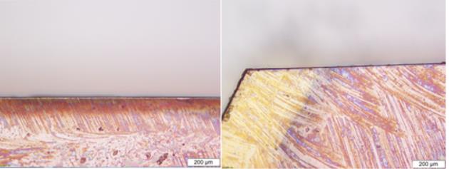
El láser de la serie FORMULA de 20W es un 40% más eficiente que el de 15W al cortar la placa FPC reforzada con un espesor de 130um, alcanzando los 140 mm/s.