Las ventajas del depanelado de corte de PCB basado en láser UV de alta potencia
Feb 07 , 2023The Advantages of high power UV Laser-Based PCB Cutting Depaneling
Technological changes in the materials, thickness, and composition of PCBs are motivating a
move away from traditional mechanical cutting and depaneling methods towards laser-based
processes. But not all lasers for PCB depaneling are created equal. There are significant
differences amongst various lasers in cut characteristics and quality, specifically in terms of
heat affected zone (HAZ). This, in turn, affects process utilization since it determines how
closely circuits can be placed on a PCB, and can also impact circuit functionality and
downstream processes like waterproofing or EMI shielding. This document presents a new
nanosecond laser and associated cutting process developed at Coherent Inc. which enables
laser PCB depaneling with substantially reduced HAZ compared to other currently available
products.
The Evolving Need for Laser Depaneling
The continued market growth of miniaturized electronic devices, including smartphones,
various wearables, VR devices, automotive sensors, and home automation equipment, to name
just a few examples, translates directly into a need for denser, higher performance PCBs. Not
only are these devices physically smaller and more complex than the previous generation of
microelectronics, there is also a consumer demand for to make them more energy efficient (for
longer battery lifetime) and less expensive.
In terms of PCB technology, this has driven several trends. Amongst these are the use of
thinner traditional boards, wide scale implementation of flex circuitry, thicker conductive layers,
and increased utilization of low-κ dielectrics (the latter especially for 5G technology). Cost
considerations also prompt a need for improved process utilization. Specifically, this translates
into placing boards closer together on a panel to increase yield.
In terms of depaneling, all this necessitates increasingly narrow kerf widths and higher
dimensional accuracy for the cutting process. Closer physical proximity of the cut to the
functional areas of the PCB also means that the cutting process must not affect the
surrounding material or circuitry, whether due to mechanical stress or heat. Minimal
production of debris, which might require a subsequent cleaning step, is another requirement.
All these constraints make traditional mechanical PCB depaneling methods, including routers,
saws, die cutting, punching, scoring, and pizza cutting, etc., less practical and less cost effective.
This impels a move towards laser cutting which offers substantial benefits in virtually every one
of the areas previously mentioned, although usually at the expense of reduced cutting speed.
Understanding Laser Cutting
Laser depaneling has, of course, been in use for some time. However, it’s important to
understand and differentiate between the various laser-based technologies. The original
implementations utilized CO2 lasers which emit in the far infrared. This technology cuts by
heating the bulk material, which results in a significant HAZ. Also, compared with shorter UV
wavelengths, this long wavelength cannot be focused to as small a spot size, meaning a larger
kerf width.
Over a decade ago, the diode-pumped solid-state (DPSS), nanosecond pulsewidth, frequencytripled laser emerged as a viable source for PCB depaneling. It offers ultraviolet (355 nm)
output with sufficient pulse energy to enable material removal through a relatively “cold”
ablation process. That is, one with a much smaller (but still noticeable) HAZ than the CO2 laser,
and also substantially less production of debris and recast material. The pulse energy and
repetition rate of commercially available sources enable cutting at economically viable feed
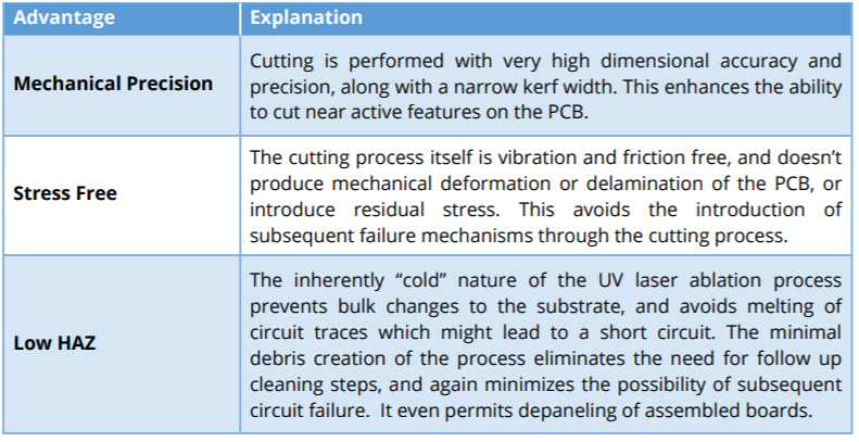
rates, although not as fast as the CO2 laser. The primary benefits of this technology are
summarized in the table.
Table 1. Primary Characteristics and Advantages of UV Laser-Based PCB Cutting

While laser depaneling clearly delivers numerous benefits, PCB manufacturers are already
pushing this technology to the limits in order to meet the ever more stringent size, materials,
and cost challenges presented by the market forces mentioned at the outset. In particular,
achieving further reductions in HAZ and debris formation, and improving the cut quality
obtained with nanosecond pulsewidth UV DPSS lasers, is an active area of development.
To aid in this effort, applications research at Coherent Inc. has explored the outcomes and
process space of using a nanosecond pulsewidth, high pulse energy, UV DPSS laser (AVIA LX) for
cutting a variety of PCB materials and material combinations. Based on this work, the Coherent
team developed a new PCB cutting method that has already proven to deliver a reduced HAZ, a
higher quality cut edge, reduced kerf width, and increased production throughput.
One key element of this technique is a proprietary method for controlling the timing and spatial
positioning of laser pulses delivered to the work surface in such a manner that heat buildup is
avoided. Because thermal damage is absent in this approach, it’s possible to utilize a laser with
substantially higher pulse energy when cutting thicker materials (1 mm and above).
The advantage of higher pulse energy is that it eliminates the need to employ the traditional
scheme used for cutting thicker materials. Specifically, this involves making a series of laterally
displaced scribes to produce a “v-groove.” The “v-groove” geometry is necessary in order to
avoid clipping the beam as it penetrates farther into the material when making a high aspect
ratio cut. This would reduce its power, and thus limit ablation efficiency. However, the AVIA LX,
coupled with this novel pulse timing approach, can utilize pulse energies as high as ~400 μJ to
repeatedly scribe along the same line (no lateral displacement, or “v-groove”). The result is
faster cutting and significantly reduced kerf width.
Higher pulse energy also increases the laser focus tolerance at the work surface. Specifically,
when using a lower pulse energy laser, it is necessary to shift the focus of the beam as the
material is penetrated so that the minimum focused spot size is always maintained precisely at
the depth at which cutting is occurring. This is necessary in order to achieve sufficient laser
fluence to get above the material ablation threshold. However, doing this in practice requires
either physically shifting the PCB up, which slows the process, or employing a three-axis
scanner (one which has a focusing capability), which increases equipment cost and complexity.
The higher pulse energy of the AVIA LX makes it possible to simply focus the laser at a point
mid-way through the PCB and perform cutting. This is because there is sufficient laser fluence
for ablation even well out of perfect focus for the laser. The benefit is faster cutting, and
reduced system complexity.
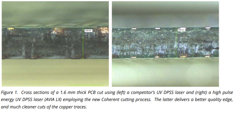
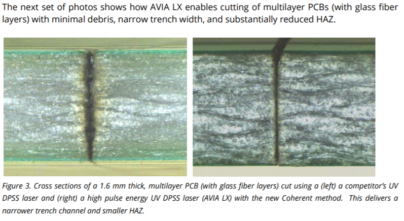
An example of the improvements are shown in the photos below, which compare cuts in a
1.6 mm thick PCB with copper traces, made using the type of UV DPSS laser currently
commercially available for this application versus the same material processed using the AVIA
LX and this new approach. The board processed with this technique shows a cleaner cut edge
and substantial improvement in the cut edges of the copper traces.
En el pasado, el corte por láser de poliimida y lámina protectora EMI producía algo de delaminación en el
línea de corte debido a la amplia ZAT. En este caso, es necesario usar una energía de pulso más baja para
evitar dañar el material. Pero, el mismo enfoque pulsante se utiliza para eliminar el calor
acumulación, y ofrece los mismos beneficios de reducción de HAZ y ancho de corte. Esto, a su vez, reduce
costos de producción al permitir que los procesos de producción posteriores alcancen mayores rendimientos.
Prácticos láseres UV DPSS de alta energía de pulso
Para materiales de PCB gruesos tradicionales, implementar el método de control de pulso Coherent en
la práctica requiere una fuente de láser UV DPSS que tenga una energía de pulso más alta que antes
comercialmente disponible. Para satisfacer esta necesidad, Coherent desarrolló el AVIA LX, un 20 W (a 355
nm), láser de ancho de pulso de nanosegundos de estado sólido, que puede producir una energía de pulso de hasta 500
µJ.
El láser AVIA LX fue diseñado específicamente para permitir PCB de alta calidad y alto rendimiento.
despanelado Combina una serie de avances tecnológicos en diseño y fabricación para
entregar esta salida de alta energía junto con una combinación inigualable de alta confiabilidad,
rendimiento superior y bajo costo de propiedad.
AVIA LX aprovecha la amplia experiencia de Coherent en la producción de
láseres con salida UV. Los cristales no lineales (tripulación de frecuencia) utilizados en el AVIA LX son
producido dentro de Coherent, lo que nos da control directo sobre la calidad y las características ópticas de
este componente crítico, y permitiéndonos lograr una vida útil más larga, un mejor rendimiento y
costo de propiedad reducido. La vida útil se maximiza aún más mediante el uso de una palanca de cambios de cristal incorporada
que contiene un mapa del cristal real en el láser y la ubicación de 20 precalificados
puntos de generación de tercer armónico (con más de 1000 horas de vida útil por punto) dentro de él.
La contaminación de la óptica es un factor limitante clave en la vida útil de los láseres UV. Láseres AVIA LX
se fabrican en una sala limpia, y las ópticas internas que están expuestas directamente a la luz ultravioleta
están contenidos dentro de un compartimento sellado PureUV para evitar la contaminación en el uso real.
Esto maximiza la vida útil y los intervalos de servicio.
Además, AVIA LX se basa en un diseño industrial extremadamente robusto, que ha sido
validado por pruebas HASS y HALT. En HALT (High Accelerated Life Testing), los prototipos se
iterativamente probado hasta la destrucción, rediseñado y vuelto a probar para eliminar cualquier inherente
debilidades HASS (detección de estrés altamente acelerado) luego estresa las unidades de producción reales
más allá de su entorno operativo especificado. Este protocolo descarta cualquier deficiencia en
fabricación y embalaje. El resultado es una fiabilidad y una vida útil inigualables del producto.
AVIA LX también está diseñado teniendo en cuenta la facilidad de integración y la facilidad de uso. Por ejemplo,
la integración se simplifica mediante el uso de electrónica de control incorporada y un expansor de haz integrado.
El uso de refrigeración por agua maximiza la vida útil y la estabilidad de pulso a pulso, incluso cuando está en funcionamiento
a alta potencia.
En conclusión, el láser Coherent AVIA LX, junto con la novedosa tecnología de control de pulsos, ha
demostró resultados superiores para el despanelado de PCB en comparación con los mecánicos tradicionales
e incluso fuentes de láser UV DPSS de ancho de pulso de nanosegundos previamente disponibles. Él
debería ser una fuente útil para una variedad de procesos de fabricación necesarios para la próxima
generación de dispositivos microelectrónicos, incluido el corte de PCB tradicionales y circuitos flexibles, SiP
corte y apertura de zanjas, y corte de blindaje EMI.