Cliente de México compra 5 unidades de fuentes UV compactas para perforar microagujeros en placas de circuito impreso
Dec 12 , 2022Mexico customer buy 5 units of compact UV sources for PCB circuit board drilling micro holes
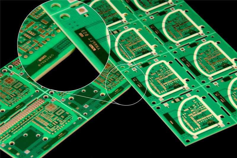
The portability and miniaturization of electronic products is the general trend, which corresponds to the miniaturization and high density of circuit boards. Electronic engineers improve the technical route plan for miniaturization of circuit boards, often by drilling holes with smaller diameters and narrower spacing on the substrate to obtain higher-density wiring space. layout and save space for higher speed, higher density boards.
The designer's wish is always beautiful, but the reality is cruel. First, due to the limitation of the material characteristics of the drill bit, the physical limit that the conventional mechanical drill bit can reach should be 0.10mm-0.15mm, which is equivalent to one-eighth of a human hair, and the manufacturing cost of the drill bit is high; There are requirements for the thickness of the board. Generally, the ratio of thickness to diameter is 1:8, that is, the thickness of the board corresponding to the hole drilled at 0.1mm is generally not more than 0.8mm. In fact, the circuit board has now expanded from single-layer boards to double-layer boards and more complex high- High-precision multilayer board; third, due to the high drilling speed of mechanical drilling, the heat generated is large, which affects the drilling efficiency to a certain extent; fourth, the axial force and cutting torque during mechanical drilling also pose challenges to the drill material , It is a test of the strength and wear resistance of the drill bit.
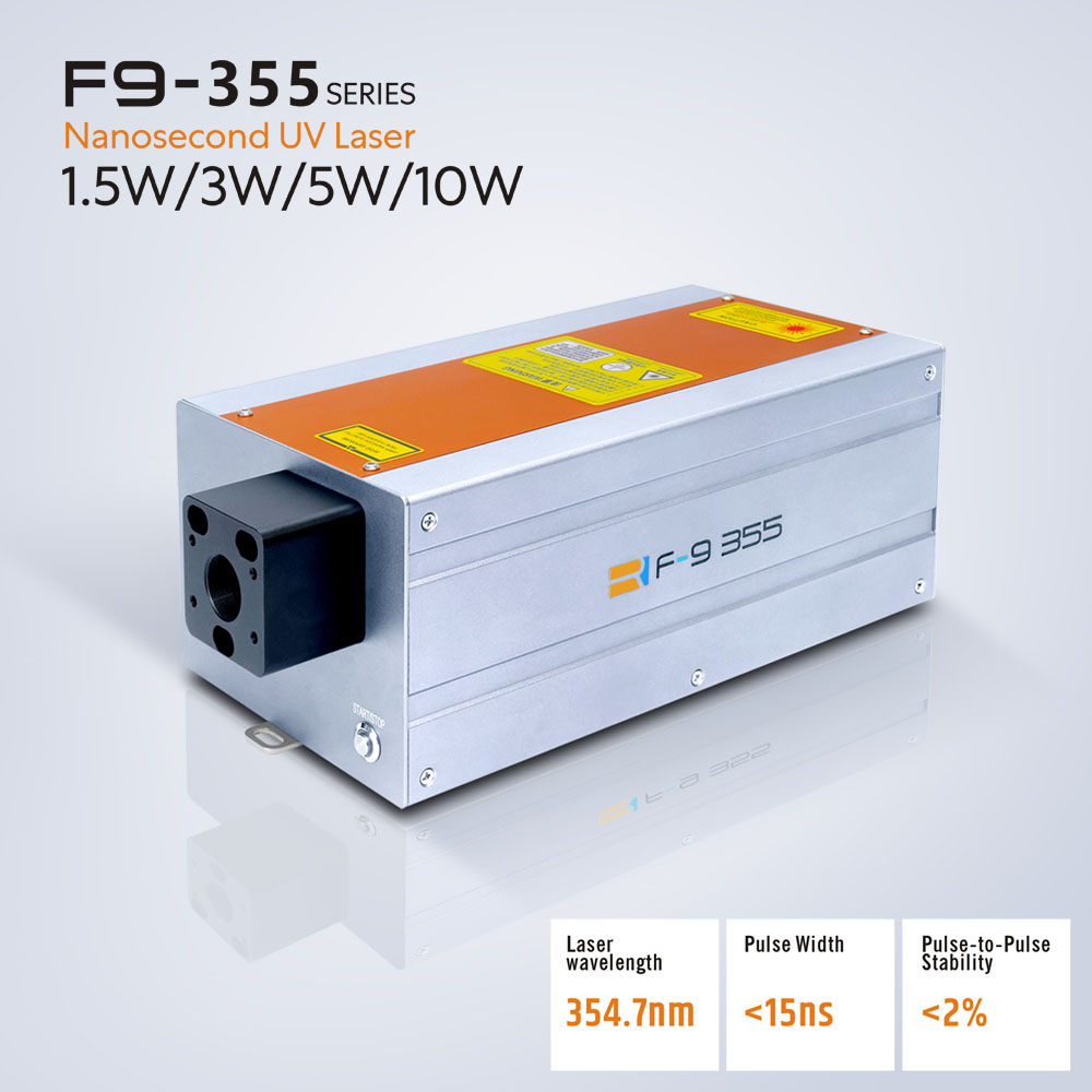
Obviamente, la perforación mecánica convencional no puede cumplir con los requisitos más altos de las placas de microcircuitos. Como un nuevo tipo de método de procesamiento, la alta colimación, la alta densidad de energía y el diámetro de punto pequeño del láser ultravioleta de nanosegundos de 355 nm pueden perforar orificios con alta precisión, alta calidad y alta eficiencia de procesamiento en la placa de circuito, lo cual está en línea con el corto tiempo de producción de la placa de circuito actual. Las características de ciclo y respuesta rápida.
El láser UV de nanosegundos de 355 nm es actualmente el láser principal para el microprocesamiento industrial. Tiene longitud de onda corta, alta tasa de absorción de material, alta energía de un solo fotón y no genera mucho calor al perforar. Este tipo de procesamiento a menudo se denomina procesamiento "en frío". , que es más fácil de obtener un mejor efecto de perforación que el tratamiento térmico de los láseres infrarrojos. Específicamente, la pared interior del orificio es lisa, el astillado del borde es pequeño y la conicidad es pequeña; además, la calidad del haz de este láser es excelente (M2<1,2), y la capacidad de enfoque es buena, el diámetro del punto después del enfoque es del orden de micras (10-20um), lo que puede cumplir con los requisitos de procesamiento de los orificios de las placas de circuitos convencionales en el mercado.